

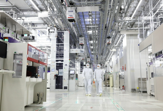
Samsung’s HBM chip packaging plant in Asan, South Korea, will drive around 40 trillion won in additional investment. President Lee Jae Myung announced the expected spending on Thursday during a groundbreaking ceremony.
The announcement follows Samsung affiliates’ investment plans unveiled in July. These plans cover projects across South Korea’s central region.
The initial investment of 6 trillion won, equivalent to around $4.48 billion, will support the new high-bandwidth memory (HBM) packaging facility.
Samsung advances HBM production timeline
Samsung Electronics plans to begin operations at the new HBM production line in June 2028. This marks an acceleration of one year from its initial schedule.
The company aims to meet rapidly growing demand for server memory. Consequently, the earlier production timeline could support its efforts to expand HBM manufacturing capacity.
According to a company presentation, the new plant will feature three floors of clean-room space. The facility will cover approximately 31,000 square metres.
South Korea backs semiconductor and AI projects
South Korea’s government has identified Samsung Electronics, SK Hynix and other companies for major investment projects.
These initiatives will cover semiconductors, physical artificial intelligence and AI data centres. Furthermore, the government aims to use these projects to strengthen the country’s advanced technology industries.
Lee’s announcement highlights the wider investment expected around Samsung’s HBM packaging expansion. The additional equipment spending will complement the initial plant investment as the company prepares for future server memory demand.